Step-by-Step Guide to the PCB Assembly Process
Have you ever wondered how all those tiny electronic parts get perfectly placed on a circuit board? The PCB assembly process might seem like magic, but it’s actually a well-organized series of steps that transforms a plain circuit board into a working electronic device. Let’s walk through this fascinating process in simple terms that anyone can understand.
What is PCB Assembly?
PCB assembly is like putting together a very complex puzzle, but instead of puzzle pieces, we’re working with electronic components. Think of it as the process where we take a bare printed circuit board (which looks like a green or blue flat board with metal lines) and carefully place all the electronic parts on it. These parts include resistors, capacitors, microchips, and many other components that make electronic devices work.
The PCB assembly process is where all the planning, designing, and component selection come together. It’s the crucial step that turns your electronic idea into a real, working device.
Why is the PCB Assembly Process So Important?
Imagine building a house – you can have the best foundation, the finest materials, and perfect blueprints, but if the construction process isn’t done properly, the house won’t be safe to live in. The same applies to electronics. Even if you have the best circuit board design and high-quality components, poor assembly can make your device unreliable or completely non-functional.
During the PCB assembly process, precision is everything. Components that are smaller than a grain of rice need to be placed exactly in the right spots. Even a tiny mistake can cause the entire device to malfunction.
Step 1: Getting Everything Ready
Before any actual assembly begins, there’s a preparation phase that’s crucial for success.
First, the bare printed circuit board arrives at the assembly facility. These boards have already gone through the fabrication process, where the copper traces and holes were created. The board is clean and ready to receive components.
Next, all the electronic components are gathered and organized. This includes everything from tiny resistors and capacitors to larger components like connectors and microprocessors. Each component is checked for quality and authenticity to make sure it will work properly.
The assembly team also prepares what’s called a Bill of Materials, or BOM for short. This is basically a detailed shopping list that tells them exactly which components go where on the board. It includes information like part numbers, quantities, and specific placement instructions.
Step 2: Applying Solder Paste
The first real assembly step involves applying something called solder paste. Solder paste is like a special glue that will eventually hold the components to the board. But not any simple glue, it’s a mixture of tiny metal particles and flux that will melt when heated and create strong electrical connections.
The solder paste is applied using a stencil, which is like a template with holes cut out in exactly the right places. The stencil is placed over the circuit board, and the paste is spread across it using a squeegee-like tool. When the stencil is removed, small dots of solder paste remain on the board exactly where components need to be placed.
This step requires incredible precision. Too much paste can cause components to slide around or create unwanted connections between different parts. Too little paste can result in weak connections that might fail later.
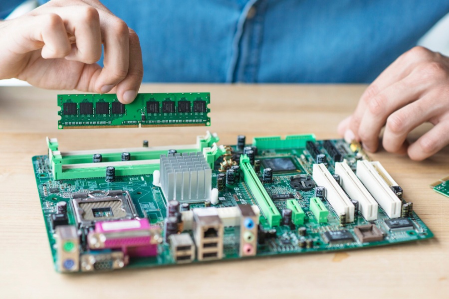
Step 3: Component Placement
This is where the magic really happens. Modern PCB assembly uses sophisticated machines that can pick up tiny components and place them on the board with amazing accuracy. These machines, called pick-and-place machines, work like incredibly precise robots.
The machine picks up each component using vacuum suction. It then positions the component exactly where it needs to go on the board, following the instructions from the Bill of Materials.
For larger components or special cases, some placement might still be done by hand by skilled technicians. This is especially true for unusual-shaped components or when very small quantities are being assembled.
The placement process covers different types of components. Some components, called Surface Mount Technology or SMT components, sit on top of the board. Others, called Through-Hole Technology or THT components, have legs that go through holes in the board.
Step 4: The Soldering Process
Once all components are in place, it’s time to make the connections permanent. This is done through soldering, which involves melting the solder paste that was applied earlier.
For SMT components, this typically involves sending the entire board through what’s called a reflow oven. This is a specialized oven that heats the board to specific temperatures in a controlled way. As the board moves through the oven, the solder paste melts and then cools down, creating strong electrical and mechanical connections between the components and the board.
For through-hole components, a different process called wave soldering might be used. In this process, the bottom of the board passes over a wave of molten solder, which flows up through the holes and around the component leads, creating solid connections.
Some manufacturers also use selective soldering for specific components that need special attention. This allows for more precise control over the soldering process for critical parts.
Step 5: Quality Inspection
After soldering, every assembled board goes through careful inspection. This is like a final quality check before the product goes to the customer.
Visual inspection is the first step, where technicians look at the board under magnification to check for obvious problems like missing components, crooked parts, or solder bridges (unwanted connections between different parts).
Many facilities also use Automated Optical Inspection (AOI), which is like having a computer with very good eyesight examine every connection on the board. The AOI system can spot problems that might be too small for human eyes to see reliably.
For more complex assemblies, X-ray inspection might be used. This is especially important for components like Ball Grid Arrays (BGAs) where the connections are hidden underneath the component. X-ray inspection can see through the component to verify that all connections are properly made.
Step 6: Testing and Final Verification
The final step in the PCB assembly process is functional testing. This is where the assembled board is powered up and tested to make sure it actually works as intended.
Basic electrical tests check things like whether power is getting to all the right places and whether there are any short circuits. More advanced functional tests might involve running the device through its intended operations to verify that everything works correctly.
Some manufacturers also perform what’s called “burn-in” testing, where the assembled boards are operated for extended periods to identify any components that might fail early in their life.
Different Types of Assembly Services
When you need PCB assembly, there are typically three different service options available:
Turnkey Assembly is like a complete package deal. The assembly company handles everything – they order all the components, test them, and assemble your board. This is convenient because you don’t have to worry about sourcing components or coordinating with multiple suppliers.
Consigned Assembly is when you provide your own components. Maybe you have special parts or prefer to source components yourself. The assembly company will test your components and then assemble them onto your boards.
Partially-Consigned Assembly is a middle ground where you provide some components and the assembly company sources the others. This might be useful if you have some specialized parts but want the assembly company to handle standard components.
Modern Assembly Capabilities
Today’s PCB assembly process can handle incredibly small components. Some components are so tiny that they’re measured in terms smaller than the width of a human hair. Modern assembly facilities can work with components as small as 01005 size, which measures just 0.016 by 0.008 inches.
The process can also handle complex components like Ball Grid Array (BGA) chips, which have hundreds of connection points arranged in a grid pattern underneath the component. These require specialized equipment and expertise to assemble correctly.
Assembly facilities can work with both traditional leaded solder and lead-free solder, depending on environmental requirements and regulations. Lead-free solder is becoming more common due to environmental concerns.
Quality Standards and Certifications
Professional PCB assembly follows strict quality standards. Many facilities are certified to international standards like ISO 9001, which ensures consistent quality management processes. For medical devices, ISO 13485 certification might be required.
The assembly process also needs to comply with various industry standards, such as IPC standards for electronic assembly. These standards specify everything from how components should be placed to what constitutes an acceptable solder joint.
Conclusion
The PCB assembly process is a fascinating blend of precision engineering and careful craftsmanship. From the initial preparation through final testing, every step requires attention to detail and quality control. Modern assembly facilities use advanced equipment and techniques to create reliable electronic devices that we use every day.
Understanding this process helps you appreciate the complexity behind even simple electronic devices. Whether you’re a student learning about electronics, an engineer developing new products, or simply curious about how things work, knowing about PCB assembly gives you insight into the world of modern manufacturing.
The next time you use your smartphone, computer, or any electronic device, remember that it all started with careful PCB assembly – tiny components precisely placed and permanently connected to create the technology that powers our modern world.